
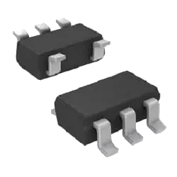
FDMS0310S Transistors - FETs, MOSFETs - Single от ON Semiconductor
FDMS0310S — это компонент категории Transistors - FETs, MOSFETs - Single от ON Semiconductor в упаковке упаковке, указанной производителем. Его обычно проверяют для MOSFET N-CH 30V 19A. На этой странице указаны текущие остатки TrustCompo, уровни цен, данные по корпусу, доступ к datasheet, compliance-атрибуты, варианты отгрузки со склада Hong Kong, подтверждение оплаты и RFQ-варианты для покупателей, которым нужно подтвердить именно этот ordering code.
Изображения приведены только для справки. Пожалуйста, свяжитесь с нами для получения последних изображений.
- Гарантия 365 днейПоддержка после покупки помогает закупщикам разбирать вопросы качества в понятный срок проверки.
- Отправка в течение 24-48 часовДоступные позиции могут быть быстро отправлены после подтверждения цены, количества и деталей доставки.
- 100% проверка на контрафактКомпоненты проходят проверку подлинности и инспекцию перед отгрузкой.
Ключевые характеристики
- Номер детали
FDMS0310S
- Внутренний код
TCE000043189
- Упаковка
-
- Производитель
- ON Semiconductor
Ключевые характеристики
- Серия
PowerTrench®, SyncFET™
- Минимальное количество
1
- Категория
- Discrete Semiconductor Products
- Подкатегория
- Transistors - FETs, MOSFETs - Single
- Описание
MOSFET N-CH 30V 19A
- Основные характеристики
-
- Техническое описание
- Открыть datasheet FDMS0310S
Сигналы доверия
Качество и доверие
Проверьте credentials TrustCompo, поддержку traceability, anti-counterfeit handling и inspection controls перед отправкой RFQ.
4 сертификата
ISO 9001
Процессы менеджмента качества для более стабильной закупки и обращения с продукцией.
AS9120B
Контроль дистрибуции авиационного уровня для прослеживаемости и надежности.
ISO 14001
Экологическая дисциплина в операционных и складских процессах.
ESD Control
Стандарты защиты от электростатического разряда для чувствительных компонентов.
RFQ checklist
Процесс заказа
Подтвердите ключевые данные закупки для FDMS0310S до RFQ, выпуска PO и планирования отгрузки.
- 1
Подтвердить MPN
Укажите точный part number, производителя, package и approval constraints в RFQ.
- 2
Проверить склад и цену
Проверьте live availability, MOQ, lead time, финальную цену и налоговые условия до PO.
- 3
Согласовать документы
Подтвердите datasheet, CoC, traceability, lifecycle notes и scope инспекции, если требуется.
- 4
Организовать отгрузку
Выпустите PO и согласуйте DHL, FedEx, UPS или buyer forwarder shipment из Hong Kong.
Перед выпуском PO
Проверка детали
- Точный MPN подтвержден: FDMS0310S
- Корпус для проверки: -
Коммерческие условия
- Live stock и срок поставки подтверждены через RFQ
- Финальная цена и налоговые условия подтверждены до выпуска PO
Отгрузка и документы
- Ship-from location: склад Hong Kong
- Способ доставки: DHL, FedEx, UPS или аккаунт экспедитора покупателя
Технические параметры
Параметры
Сравните сгруппированные параметры FDMS0310S от ON Semiconductor, включая package, series, key attributes и technical values для engineering и sourcing review.
Product Parameter
Terminal Finish
Tin (Sn)
Product Parameter
Number of Channels
2
Product Parameter
Number of Elements
1
Product Parameter
Drain to Source Voltage (Vdss)
30V
Product Parameter
Turn On Delay Time
12 ns
Product Parameter
Turn-Off Delay Time
28 ns
| Параметр | Значение |
|---|---|
Terminal Finish Specifies the plating material on component terminals, affecting solderability, corrosion resistance, and long-term reliability. Compare finishes like tin, gold, or silver for your assembly process and environmental requirements. Verify against datasheet for compliance. | Tin (Sn) |
Number of Channels Specifies how many independent signal paths or outputs the component provides. Compare this value with your circuit requirements to ensure each channel can be used separately. Verify the channel configuration in the datasheet, as some devices may share pins or have internal connections. | 2 |
Number of Elements Indicates how many independent functional sections are integrated into a single component package. This matters when comparing multi-channel devices or resistor networks. Always verify the exact element count against the datasheet to ensure it matches your circuit design requirements. | 1 |
Drain to Source Voltage (Vdss) Maximum voltage that can be applied between drain and source terminals without causing breakdown. Critical for MOSFET selection in power circuits. Verify against datasheet for safe operating area and derating. | 30V |
Turn On Delay Time Time from when the input signal crosses its threshold until the output begins to turn on. This parameter affects switching speed and power dissipation in high-frequency circuits. Verify it against the datasheet for your specific load and drive conditions. | 12 ns |
Turn-Off Delay Time Measures the time from when the turn-off command is applied to when the device actually begins to switch off. This delay affects switching losses and timing in power circuits. Engineers compare this parameter to ensure proper synchronization and to minimize power dissipation during high-frequency operation. | 28 ns |
Rise Time Time required for a signal to transition from a low to a high level, typically measured between 10% and 90% of the amplitude. Important for digital interfaces, switching regulators, and pulse circuits. Check the datasheet for test conditions and load capacitance. | 5ns |
| Параметр | Значение |
|---|---|
Part Status Lifecycle status of the part, such as active or obsolete. Indicates availability and long-term support from the manufacturer. Check this before design-in to avoid last-time buys or supply disruptions. Verify with the datasheet or distributor for current status. | Active |
REACH Status Shows whether the component complies with the EU REACH regulation. Essential for legal market access in Europe. Check the manufacturer's latest statement to confirm that no substances of very high concern are present above the threshold. | REACH Unaffected |
ECCN Export Control Classification Number assigned by the U.S. government. Determines whether the component requires an export license. Essential for international trade compliance. Verify the ECCN with the manufacturer or supplier before shipping to avoid legal issues. | EAR99 |
Lifecycle Status Current stage in the product's lifecycle, such as Active, Obsolete, or End of Life. This indicates availability and long-term supply risk. Check this before designing in a part to ensure it will be available for your product's production lifetime. | ACTIVE (Last Updated: 2 days ago) |
Mounting Type Specifies how the component is attached to the PCB, such as through-hole or surface mount. This affects assembly processes, thermal performance, and mechanical strength. Buyers should verify compatibility with their manufacturing capabilities and design requirements. | Surface Mount |
Published Published indicates the date when the product data was released or updated in the catalog. It helps buyers assess the freshness of the information and whether the component is current or possibly obsolete. Check the datasheet for the latest revisions. | 2006 |
Packaging Indicates the form of delivery for the component, such as tape and reel, tube, or tray. This affects handling, storage, and assembly processes. Verify the packaging type matches your production requirements and equipment compatibility. | Tape & Reel (TR) |
Factory Lead Time Indicates the typical duration from order confirmation to shipment from the manufacturer's facility. This helps you plan production schedules and inventory. Verify current lead times with your distributor or supplier, as they may vary based on order quantity, product availability, and market conditions. | 18 Weeks |
Terminal Position Position of the terminals on the package, such as dual-in-line, gull-wing, or J-lead. This affects PCB layout, soldering, and thermal performance. Engineers must ensure the terminal position matches the footprint and assembly capabilities of their manufacturing line. | DUAL |
REACH Compliance Code Indicates the component's compliance status with the EU REACH regulation. Buyers should verify this code against the manufacturer's declaration to ensure restricted substances are within allowable limits for their target market. | not_compliant |
Element Configuration Describes the internal arrangement of components, such as resistor networks or switch contacts. This affects the circuit topology and pinout. Engineers must verify this configuration against the datasheet to ensure correct integration into the PCB layout and proper functionality. | Single |
Manufacturer Identifies the company that designed and produced the component. Buyers often filter by manufacturer to ensure brand reliability, quality standards, and supply chain consistency. Verify the manufacturer against the datasheet and official packaging to avoid counterfeit parts. | ON Semiconductor |
Case Connection Indicates how the component's case or package is electrically connected, such as to ground, a supply rail, or left floating. This affects thermal management, shielding, and circuit isolation. Always confirm with the datasheet to ensure proper PCB layout and avoid unintended shorts or noise coupling. | DRAIN |
Operating Mode Specifies the functional mode of the component, such as continuous, pulsed, or burst. Engineers compare this to ensure the device operates correctly in their circuit topology. Verify the mode against the datasheet to match your application's requirements. | ENHANCEMENT MODE |
Subcategory A more specific classification within the main product category, such as 'Ceramic Capacitor' under 'Capacitors'. This helps narrow down search results and compare similar components. Use it to filter products with similar characteristics and intended applications. | FET General Purpose Power |
Technology Manufacturing technology or process used for the component, such as thin film, thick film, or semiconductor process. Affects performance, stability, and cost. Confirm the technology matches your application requirements and environmental conditions. | MOSFET (Metal Oxide) |
FET Type Classification of field-effect transistor based on channel polarity and mode, such as N-channel or P-channel, enhancement or depletion. This determines the required gate drive polarity and circuit topology. Engineers select the appropriate type for switching or amplification applications. Always confirm the exact type from the datasheet before design. | N-Channel |
Sub-Categories Indicates the specific product subcategories or classifications within the broader component family. Helps narrow down search results and identify the exact type of component needed for your design. Review the subcategory to ensure compatibility with your application. | Transistors - FETs, MOSFETs - Single |
Vgs (Max) Maximum allowable gate-to-source voltage for a MOSFET. Exceeding this rating can permanently damage the gate oxide. Check the datasheet's absolute maximum ratings and ensure your drive circuit stays within this limit under all conditions. | ±20V |
Categories Lists the product categories or classifications assigned to this component, such as connectors, capacitors, or modules. This helps in filtering and comparing similar parts. Review the categories to ensure the component fits your application and to find alternative parts in the same class. | Discrete Semiconductor Products |
Transistor Application Specifies the intended circuit role, such as switching, amplification, or RF. Engineers compare this to ensure the transistor's characteristics match the design's requirements. Verify against the datasheet's application section before selecting. | SWITCHING |
Transistor Element Material Specifies the semiconductor material used in the transistor's active region. This affects electrical characteristics such as switching speed and voltage rating. Verify the material against the datasheet when selecting for high-frequency or high-power applications. | SILICON |
Operating Temperature Specifies the ambient temperature range within which the component reliably functions. Compare this with your application's thermal environment to ensure proper operation. Always verify against the datasheet for derating curves and maximum ratings. | -55°C~150°C TJ |
Drive Voltage (Max Rds On, Min Rds On) Gate-to-source voltage levels that produce the specified maximum and minimum on-resistance values. This helps designers select appropriate gate drive circuits and logic levels. Check the datasheet's transfer characteristics to ensure the MOSFET fully enhances at your operating voltage. | 4.5V 10V |
Package / Case Physical package or case type of the component, defining its dimensions, mounting style, and thermal characteristics. Common types include SMD, through-hole, BGA, and QFN. Choose the package that fits your PCB layout and assembly process. Verify the exact package code in the datasheet for footprint compatibility. | 8-PowerTDFN |
Mounting Type Specifies how the component attaches to the PCB or assembly, such as surface mount, through-hole, or chassis mount. This affects soldering process, mechanical stability, and thermal performance. Verify compatibility with your board layout and assembly capabilities. | Surface Mount |
Pb-Free Code Indicates whether the component is lead-free per RoHS or other directives. Buyers use this to verify environmental compliance and avoid restricted substances. Always confirm with the datasheet or certificate of compliance. | yes |
Number of Terminations Indicates the total number of electrical connection points on the component, such as pins or pads. This is critical for PCB footprint design and assembly. Verify it matches the package specification to ensure proper soldering and connectivity. | 5 |
Number of Pins Total number of pins or contacts on the component. This determines the footprint and mating connector requirements. Always match the pin count to your PCB layout and connector specification to ensure proper electrical and mechanical connection. | 8 |
Terminal Form Describes the physical configuration of the component's leads or pads, such as through-hole, surface mount, or gull-wing. This affects PCB layout, soldering process, and mechanical fit. Confirm compatibility with your assembly method and footprint. | FLAT |
Peak Reflow Temperature (Cel) Maximum temperature during reflow soldering that the component can withstand. This is critical for solder joint reliability and preventing damage. Verify that the peak reflow temperature is compatible with your soldering profile and the component's moisture sensitivity level. | NOT SPECIFIED |
Gate to Source Voltage (Vgs) Voltage applied between gate and source terminals that controls the MOSFET's conduction. This rating defines the absolute maximum allowable voltage to prevent gate oxide breakdown. Check the threshold voltage and recommended drive levels in the datasheet for reliable switching. | 20V |
Reflow Temperature-Max (s) Maximum time the component can be exposed to the peak reflow temperature during soldering. Exceeding this duration may cause damage or degrade reliability. Ensure your soldering profile stays within this limit and check the datasheet for exact conditions. | NOT SPECIFIED |
Weight Specifies the physical weight of the electronic component, important for logistics, shipping cost, and mechanical design. Verify the exact weight in the datasheet or packaging information, as it may vary with packaging type and quantity. | 68.1mg |
Height Physical height of the component, measured from the mounting surface to the topmost point. This dimension is critical for clearance in compact assemblies and for ensuring proper fit within enclosures. Always verify against the datasheet for tolerance and mounting considerations. | 1mm |
Width Physical width of the component body, typically in millimeters. Essential for PCB footprint design and mechanical fit. Verify against the datasheet to ensure proper clearance and compatibility with your board layout and enclosure. | 5mm |
Length Specifies the physical length of the component body, typically in millimeters. This dimension is critical for PCB layout and mechanical fit. Verify against the datasheet to ensure proper clearance and alignment in your design. | 6mm |
Continuous Drain Current (ID) Maximum continuous current the MOSFET can conduct in the on-state without exceeding thermal limits. Compare this rating with your circuit's peak and average current demands. Always verify against the datasheet's thermal resistance and ambient temperature conditions. | 42A |
Drain Current-Max (Abs) (ID) Absolute maximum continuous drain current the MOSFET can handle without damage. Compare this rating against your circuit's peak current demand. Always verify with the datasheet's safe operating area and thermal limits. | 19A |
Pulsed Drain Current-Max (IDM) Maximum drain current under pulsed conditions, often specified with a pulse width and duty cycle. Compare this value with the continuous drain current rating to understand the device's peak current capability. Verify the pulse conditions in the datasheet to ensure they match your application's switching requirements. | 90A |
Vgs(th) Max @ Id Maximum gate threshold voltage at a specified drain current. This parameter indicates the gate voltage needed to begin conduction. Compare it with your gate drive voltage to ensure reliable switching. Verify against the datasheet for your operating conditions. | 3V @ 1mA |
Fall Time (Typ) Typical time for the output signal to transition from 90% to 10% of its amplitude. This parameter indicates switching speed and affects high-frequency performance. Compare with rise time and verify against the datasheet for your specific operating conditions. | 4 ns |
Avalanche Energy Rating (Eas) Maximum energy the device can absorb during a single avalanche event without failure. Compare this rating when designing inductive load switching or surge conditions. Verify against the datasheet to ensure your circuit's energy stress stays within safe limits. | 60 mJ |
Gate Charge (Qg) (Max) @ Vgs This is the total charge required to switch the MOSFET gate to a specified gate-source voltage. It determines switching speed and driver power losses. Compare values to optimize efficiency in high-frequency circuits. Verify against datasheet for your operating conditions. | 46nC @ 10V |
DS Breakdown Voltage-Min Minimum drain-to-source breakdown voltage for MOSFETs. This value indicates the maximum voltage the device can block in the off-state. Engineers compare it with the operating voltage to ensure sufficient safety margin. Always verify against the datasheet for the specific test conditions. | 30V |
Series Indicates the product series or family, grouping components with similar design and specifications. Helps identify compatible parts and compare within a product line. Verify the series against the datasheet to ensure correct application. | PowerTrench®, SyncFET™ |
Maximum Power Dissipation Indicates the highest power the component can safely dissipate as heat without exceeding its thermal limits. Compare this value with your circuit's expected power loss to ensure reliable operation. Always verify against the datasheet's derating curves for elevated ambient temperatures. | 2.5W Ta 46W Tc |
Manufacturer's Part No. The unique part number assigned by the original component manufacturer. Use this to cross-reference datasheets, verify specifications, and ensure the exact component matches your design requirements. Always confirm the number against the manufacturer's official documentation. | FDMS0310S |
Rds On (Max) @ Id, Vgs Maximum drain-source on-resistance measured at a specified drain current and gate-source voltage. Lower values reduce conduction losses in power circuits. Compare this parameter when selecting MOSFETs for efficiency and thermal performance, and verify against the datasheet. | 4m Ω @ 18A, 10V |
Input Capacitance (Ciss) (Max) @ Vds Maximum input capacitance of the MOSFET at a specified drain-source voltage. This value affects switching speed and gate drive requirements. Compare across devices to estimate switching losses and driver capability. Always verify against the datasheet for your operating conditions. | 2820pF @ 15V |
Drain-source On Resistance-Max Maximum on-state resistance between drain and source for MOSFETs when fully enhanced. This parameter affects power dissipation and efficiency in switching applications. Lower resistance reduces losses and heat. Compare this value with your current requirements and check the gate drive voltage in the datasheet. | 0.004Ohm |
Continuous Drain Current (Id) @ 25°C Maximum continuous current the MOSFET can conduct at 25°C case temperature. This rating determines thermal performance and suitability for power applications. Verify against the datasheet's safe operating area and derating curves for reliable operation. | 19A Ta 42A Tc |
| Параметр | Значение |
|---|---|
JESD-609 Code This code indicates the terminal finish material per JESD-609 standard. It helps identify the plating type for soldering compatibility and environmental compliance. Check the datasheet for the exact code and its meaning. | e3 |
Moisture Sensitivity Level (MSL) Indicates the floor life of a component before it must be baked prior to soldering. Higher levels require stricter handling and shorter exposure times. Verify the MSL rating in the datasheet to ensure proper storage and assembly conditions. | 1 (Unlimited) |
RoHS Status Indicates whether the component complies with the EU RoHS directive restricting hazardous substances. Buyers should verify this status for regulatory compliance and market access. Check the datasheet or certificate for exact compliance details. | ROHS3 Compliant |
HTSUS Harmonized Tariff Schedule of the United States code for customs classification. Essential for import/export documentation and duty calculation. Verify the correct code with a trade specialist to avoid customs delays. | 8541.29.0095 |
ECCN Code Export Control Classification Number assigned by the U.S. Commerce Department. It determines export licensing requirements for electronic components. Verify the ECCN against the manufacturer's datasheet or export compliance documentation before shipping internationally. | EAR99 |
JESD-30 Code JEDEC standard code that defines the package outline and dimensions. Use it to verify physical compatibility and footprint before PCB design. Compare with the datasheet to ensure the component meets your assembly and manufacturing requirements. | R-PDSO-F5 |
Предпросмотр datasheet
Datasheet PDF viewer
Просмотрите datasheet для FDMS0310S от ON Semiconductor, чтобы проверить package, electrical characteristics, application notes и document evidence до RFQ.
ON Semiconductor
FDMS0310S
Страница 1 из 0 / —
Загрузка PDF viewer...
Документы уведомлений
PCN / product notice documents
0 документов
Публичные PCN / PDN записи сейчас не показаны
Для FDMS0310S сейчас не показан публичный product notice document. Подтвердите PCN, PDN, EOL, date code и lifecycle status во время RFQ до производственной закупки.
Связанные варианты закупки
Рекомендуемые товары
Посмотрите больше компонентов из той же подкатегории, чтобы сравнить наличие, совместимость и варианты закупки.
Частые вопросы
FAQ по товару
Точные ответы для покупателей, которые проверяют ordering code FDMS0310S, упаковку, наличие, datasheet и путь замены.
Что означает FDMS0310S?
FDMS0310S — это точный ordering code для компонента категории Transistors - FETs, MOSFETs - Single от ON Semiconductor. Текущий корпус указан как -, а контекст позиции включает MOSFET N-CH 30V 19A. Используйте полный код при запросе склада, цены, datasheet или compliance-подтверждения.
Как покупателям проверить ordering code FDMS0310S?
Рассматривайте FDMS0310S как полный ordering code при RFQ и инженерной проверке. Подтвердите указанный корпус -, документацию производителя ON Semiconductor, ordering table в datasheet, reel или packing details и требования внутреннего утверждения до замены или выпуска PO.
В каком корпусе поставляется FDMS0310S?
FDMS0310S сейчас указан с корпусом - от ON Semiconductor. Перед утверждением закупки подтвердите manufacturer package drawing, footprint, pinout, tape-and-reel данные и требования к приемке.
FDMS0310S сейчас доступен для заказа?
FDMS0310S сейчас помечен на странице как позиция с наличием. Перед заказом подтвердите корпус (-), указанный склад (98776), доступное количество (48286), нужное количество, срок поставки, финальную цену, compliance-требования и совпадение точного ordering code через RFQ.
Где сравнить альтернативы для FDMS0310S?
Для FDMS0310S сейчас не опубликован список связанных альтернатив. Отправьте RFQ с количеством, ограничениями по корпусу и требованиями к утверждению, чтобы TrustCompo помогла проверить возможные replacement options.