
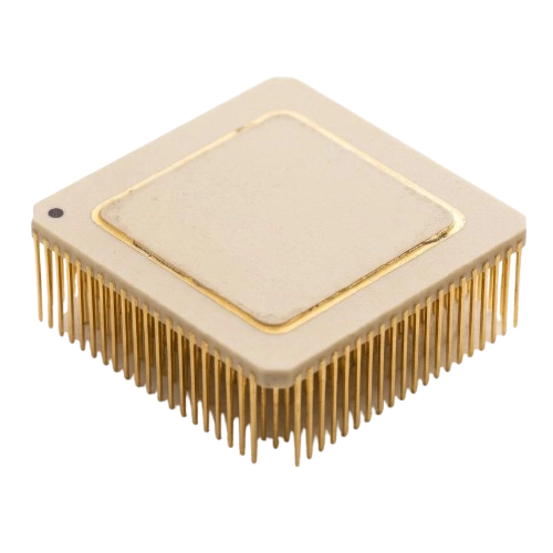
XC2S100-5FG256C Embedded - FPGAs (Field Programmable Gate Array) от Xilinx
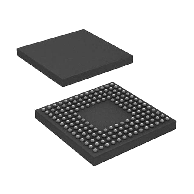
XC2S100-5FG256C — это компонент категории Embedded - FPGAs (Field Programmable Gate Array) от Xilinx в упаковке BGA. Его обычно проверяют для IC FPGA 176 I/O 256FBGA. На этой странице указаны текущие остатки TrustCompo, уровни цен, данные по корпусу, доступ к datasheet, compliance-атрибуты, варианты отгрузки со склада Hong Kong, подтверждение оплаты и RFQ-варианты для покупателей, которым нужно подтвердить именно этот ordering code.
В наличииDatasheet
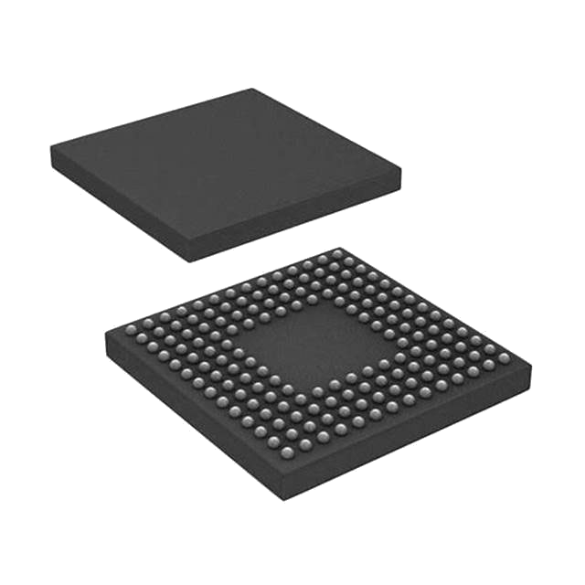
Изображения приведены только для справки. Пожалуйста, свяжитесь с нами для получения последних изображений.
- Гарантия 365 днейПоддержка после покупки помогает закупщикам разбирать вопросы качества в понятный срок проверки.
- Отправка в течение 24-48 часовДоступные позиции могут быть быстро отправлены после подтверждения цены, количества и деталей доставки.
- 100% проверка на контрафактКомпоненты проходят проверку подлинности и инспекцию перед отгрузкой.
Ключевые характеристики
- Номер детали
XC2S100-5FG256C
- Внутренний код
TCE000120684
- Упаковка
BGA
- Производитель
- Xilinx
Ключевые характеристики
- Серия
Spartan®-II
- Минимальное количество
1
- Категория
- Integrated Circuits (ICs)
- Подкатегория
- Embedded - FPGAs (Field Programmable Gate Array)
- Описание
IC FPGA 176 I/O 256FBGA
- Основные характеристики
-
- Техническое описание
- Открыть datasheet XC2S100-5FG256C
Сигналы доверия
Качество и доверие
Проверьте credentials TrustCompo, поддержку traceability, anti-counterfeit handling и inspection controls перед отправкой RFQ.
4 сертификата
ISO 9001
Процессы менеджмента качества для более стабильной закупки и обращения с продукцией.
AS9120B
Контроль дистрибуции авиационного уровня для прослеживаемости и надежности.
ISO 14001
Экологическая дисциплина в операционных и складских процессах.
ESD Control
Стандарты защиты от электростатического разряда для чувствительных компонентов.
RFQ checklist
Процесс заказа
Подтвердите ключевые данные закупки для XC2S100-5FG256C до RFQ, выпуска PO и планирования отгрузки.
- 1
Подтвердить MPN
Укажите точный part number, производителя, package и approval constraints в RFQ.
- 2
Проверить склад и цену
Проверьте live availability, MOQ, lead time, финальную цену и налоговые условия до PO.
- 3
Согласовать документы
Подтвердите datasheet, CoC, traceability, lifecycle notes и scope инспекции, если требуется.
- 4
Организовать отгрузку
Выпустите PO и согласуйте DHL, FedEx, UPS или buyer forwarder shipment из Hong Kong.
Перед выпуском PO
Проверка детали
- Точный MPN подтвержден: XC2S100-5FG256C
- Корпус для проверки: BGA
Коммерческие условия
- Live stock и срок поставки подтверждены через RFQ
- Финальная цена и налоговые условия подтверждены до выпуска PO
Отгрузка и документы
- Ship-from location: склад Hong Kong
- Способ доставки: DHL, FedEx, UPS или аккаунт экспедитора покупателя
Обзор продукта
Обзор
Проверьте sourcing context для XC2S100-5FG256C от Xilinx, включая идентификацию товара, применимость, package notes и закупочные детали.
Description
The XC226x derivatives are high-performance members of the Infineon XC2000 Family of full featured single-chip CMOS microcontrollers.
These devices extend the functionality and performance of the C166 Family in terms of instructions (MAC unit), peripherals, and speed.
They combine high CPU performance (up to 66 million instructions per second) with high peripheral functionality and enhanced IO-capabilities. Optimized peripherals can be adapted to the application’s requirements in a flexible way.
These derivatives also provide clock generation via PLL and internal or external clock sources, and various on-chip memory modules such as program Flash, program RAM, and data RAM.
Features
For a quick overview or reference, the XC226x’s properties are listed here in a condensed way.
• High Performance 16-bit CPU with 5-Stage Pipeline– 15 ns Instruction Cycle Time at 66 MHz CPU Clock (Single-Cycle Execution)– 1-Cycle 32-bit Addition and Subtraction with 40-bit result– 1-Cycle Multiplication (16 × 16 bit)– 1-Cycle Multiply-and-Accumulate (MAC) Instructions– Background Division (32 / 16 bit) in 21 Cycles– Enhanced Boolean Bit Manipulation Facilities– Zero-Cycle Jump Execution– Additional Instructions to Support HLL and Operating Systems– Register-Based Design with Multiple Variable Register Banks– Fast Context Switching Support with Two Additional Local Register Banks– 16 Mbytes Total Linear Address Space for Code and Data– 1024 Bytes On-Chip Special Function Register Area (C166 Family Compatible)
• 16-Priority-Level Interrupt System with up to 87 Sources, Selectable External Inputsfor Interrupt Generation and Wake-Up, Sample-Rate down to 15 ns
• 8-Channel Interrupt-Driven Single-Cycle Data Transfer Facilities viaPeripheral Event Controller (PEC), 24-Bit Pointers Cover Total Address Space
• Clock Generation from Internal or External Clock Sources,via on-chip PLL or via Prescaler
• On-Chip Memory Modules– 1 Kbyte On-Chip Stand-By RAM (SBRAM)– 2 Kbytes On-Chip Dual-Port RAM (DPRAM)– 16 Kbytes On-Chip Data SRAM (DSRAM)– Up to 64 Kbytes On-Chip Program/Data SRAM (PSRAM)– Up to 768 Kbytes On-Chip Program Memory (Flash Memory)
• On-Chip Peripheral Modules– Two Synchronizable A/D Converters with a total of 16 Channels, 10-bit Resolution,Conversion Time down to 1.2 µs, Optional Data Preprocessing (Data Reduction,Range Check)– 16-Channel General Purpose Capture/Compare Unit (CAPCOM2)– Up to four Capture/Compare Units for flexible PWM Signal Generation (CCU6x)– Multi-Functional General Purpose Timer Unit with 5 Timers– Six Serial Interface Channels to be used as UART, LIN, High-Speed SynchronousChannel (SPI/QSPI), IIC Bus Interface (10-bit addressing, 400 kbit/s), IIS Interface– On-Chip MultiCAN Interface (Rev. 2.0B active) with up to 128 Message Objects(Full CAN/Basic CAN) on up to 5 CAN Nodes and Gateway Functionality– On-Chip Real Time Clock
• Up to 12 Mbytes External Address Space for Code and Data– Programmable External Bus Characteristics for Different Address Ranges– Multiplexed or Demultiplexed External Address/Data Buses– Selectable Address Bus Width– 16-Bit or 8-Bit Data Bus Width– Four Programmable Chip-Select Signals
• Single Power Supply from 3.0 V to 5.5 V
• Power Reduction Modes with Flexible Power Management
• Programmable Watchdog Timer and Oscillator Watchdog
• Up to 75 General Purpose I/O Lines
• On-Chip Bootstrap Loader
• Supported by a Large Range of Development Tools like C-Compilers,Macro-Assembler Packages, Emulators, Evaluation Boards, HLL-Debuggers, Simulators,Logic Analyzer Disassemblers, Programming Boards
• On-Chip Debug Support via JTAG Interface
• 100-Pin Green LQFP Package, 0.5 mm (19.7 mil) pitch
Технические параметры
Параметры
Сравните сгруппированные параметры XC2S100-5FG256C от Xilinx, включая package, series, key attributes и technical values для engineering и sourcing review.
Product Attribute
Categories
Integrated Circuits (ICs)
Product Attribute
Terminal Position
Surface Mount
Product Attribute
Max Supply Voltage
Surface Mount
Product Attribute
Converter Type
3 (168 Hours)
Product Attribute
Package / Case
256-BGA
Product Attribute
Housing Material
Non-RoHS Compliant
| Параметр | Значение |
|---|---|
Categories Lists the product categories or classifications assigned to this component, such as connectors, capacitors, or modules. This helps in filtering and comparing similar parts. Review the categories to ensure the component fits your application and to find alternative parts in the same class. | Integrated Circuits (ICs) |
Terminal Position Position of the terminals on the package, such as dual-in-line, gull-wing, or J-lead. This affects PCB layout, soldering, and thermal performance. Engineers must ensure the terminal position matches the footprint and assembly capabilities of their manufacturing line. | Surface Mount |
Max Supply Voltage Indicates the highest DC or AC voltage that can be safely applied to the power supply pin without risking damage or malfunction. Verify this limit against the datasheet before designing your circuit to ensure reliable operation under all conditions. | Surface Mount |
Converter Type Identifies the conversion architecture, such as ADC, DAC, or DC-DC. This determines the signal path, interface, and performance characteristics. Verify the type matches your system's analog or digital conversion needs before selecting the part. | 3 (168 Hours) |
Package / Case Physical package or case type of the component, defining its dimensions, mounting style, and thermal characteristics. Common types include SMD, through-hole, BGA, and QFN. Choose the package that fits your PCB layout and assembly process. Verify the exact package code in the datasheet for footprint compatibility. | 256-BGA |
Housing Material Specifies the material of the component's outer casing, such as plastic, metal, or ceramic. This affects durability, thermal performance, and environmental resistance. Verify against datasheet for application-specific requirements like flammability or chemical exposure. | Non-RoHS Compliant |
Locking Feature Indicates the locking mechanism used to secure the connector or terminal in place. Choose the appropriate type for your application to ensure reliable mating and vibration resistance. Verify compatibility with the mating part and datasheet specifications. | Contains Lead |
Interface Type Specifies the communication protocol used by the component to exchange data with a host controller or other devices. Common examples include I2C, SPI, UART, USB, and CAN. Verify compatibility with your system's bus architecture and voltage levels before integration. | not_compliant |
Sub-Categories Indicates the specific product subcategories or classifications within the broader component family. Helps narrow down search results and identify the exact type of component needed for your design. Review the subcategory to ensure compatibility with your application. | Embedded - FPGAs (Field Programmable Gate Array) |
Supply Voltage Specifies the nominal operating voltage that must be applied to the component for proper function. Verify this value against your system's power rail and the datasheet's absolute maximum ratings to ensure reliable operation and avoid damage. | 1999 |
Input Power-Max (CW) Indicates the maximum continuous wave input power the component can safely handle without damage or excessive distortion. Exceeding this limit may cause failure. Verify this value against your signal power and consider peak-to-average ratio in modulated systems. | 10 Weeks |
Resistance Electrical resistance value in ohms, defining opposition to current flow. Critical for current limiting, voltage division, and signal conditioning. Always check tolerance and power rating in the datasheet for reliable circuit operation. | 2.5V |
Manufacturer Identifies the company that designed and produced the component. Buyers often filter by manufacturer to ensure brand reliability, quality standards, and supply chain consistency. Verify the manufacturer against the datasheet and official packaging to avoid counterfeit parts. | Xilinx |
Radiation Hardening Indicates if the component is designed to withstand ionizing radiation in space, nuclear, or high-energy physics applications. Compare radiation-tolerant vs. radiation-hardened parts for mission-critical designs. Verify the total ionizing dose (TID) and single-event effect (SEE) ratings in the datasheet. | 0°C~85°C TJ |
Specifications Review the complete technical specifications for this electronic component, including electrical ratings, mechanical dimensions, and environmental limits. Verify these parameters against your application requirements and the manufacturer's datasheet to ensure compatibility and reliable operation. | Tin/Lead (Sn63Pb37) |
Number of I/O Total number of input/output pins or channels available on the device. Determines connectivity and interface capability. Verify against your system requirements and datasheet to ensure sufficient I/O for your application. | 176 |
Temperature Grade Defines the operating temperature range classification for the component, such as commercial, industrial, or automotive. This indicates the environmental conditions the device can withstand. Ensure the grade matches your application's ambient temperature requirements. | 256 |
Threshold Voltage The minimum gate-to-source voltage that makes the device start conducting. Compare this value across parts to ensure your drive circuit can reliably turn the switch on. Always verify against the datasheet for your operating temperature. | 17mm |
Data Rate Specifies the maximum data transfer rate the component can handle, typically in bits per second. Compare this value with your system's required throughput to ensure adequate bandwidth. Verify against the datasheet for exact conditions and supported protocols. | 256 |
Series Indicates the product series or family, grouping components with similar design and specifications. Helps identify compatible parts and compare within a product line. Verify the series against the datasheet to ensure correct application. | Spartan®-II |
Mounting Type Specifies how the component attaches to the PCB or assembly, such as surface mount, through-hole, or chassis mount. This affects soldering process, mechanical stability, and thermal performance. Verify compatibility with your board layout and assembly capabilities. | 263MHz |
Bus Directional Indicates whether the bus supports data flow in one direction only or in both directions. This affects signal routing and buffer design. Verify against the datasheet to ensure compatibility with your system's communication requirements. | 0.7 ns |
Temperature Coefficient Indicates how much a key parameter, such as voltage or resistance, changes per degree Celsius. Lower values mean better stability across temperature. Verify this against your operating temperature range to ensure consistent performance in your environment. | 2.375V~2.625V |
Technology Manufacturing technology or process used for the component, such as thin film, thick film, or semiconductor process. Affects performance, stability, and cost. Confirm the technology matches your application requirements and environmental conditions. | XC2S100 |
Manufacturer's Part No. The unique part number assigned by the original component manufacturer. Use this to cross-reference datasheets, verify specifications, and ensure the exact component matches your design requirements. Always confirm the number against the manufacturer's official documentation. | XC2S100-5FG256C |
Programmable Flags Support Indicates whether the device supports user-configurable flags for status or control. Check the datasheet to see which flags are programmable and how they behave during operation. | 600 |
| Параметр | Значение |
|---|---|
Triac Type Specifies the triac construction or series, such as standard, snubberless, or logic-level. This affects switching performance, gate sensitivity, and commutation capability. Verify the exact type against the datasheet to ensure compatibility with your circuit's voltage, current, and triggering requirements. | Active |
Typical Quiescent Current (mA) Typical current consumed by the component in standby or idle state, measured in milliamperes. This is important for battery-powered or low-power applications. Compare this value with your power budget to ensure the component does not drain excessive current when inactive, affecting overall system efficiency. | CMOS |
Drain to Source Resistance This is the on-state resistance between the drain and source terminals of a MOSFET. It affects power dissipation and efficiency. Lower values are preferred for high-current switching. Always check the datasheet for the specified test conditions, as RDS(on) varies with gate voltage and temperature. | EAR99 |
On-state Resistance Match-Nom Indicates the nominal matching of on-state resistance between multiple channels in a device, such as a dual MOSFET or analog switch. This parameter is critical for parallel operation and current sharing. Verify the specified match against the datasheet to ensure balanced performance. | Not Qualified |
Transformer Type Indicates the construction or configuration of the transformer, such as flyback, forward, or planar. Affects performance, size, and application suitability. Refer to datasheet for detailed specifications and recommended usage. | no |
Total Resistance Total resistance is the end-to-end resistance of a component, such as a potentiometer or resistor network. It defines the maximum resistance available and is critical for circuit design. Verify this value against the datasheet to ensure proper operation. | Tray |
Transmission Media Type Specifies the physical medium through which signals travel, such as fiber optic, twisted pair, or coaxial cable. This attribute is critical for ensuring compatibility with your network infrastructure and for meeting performance requirements. Verify the media type against your system's specifications and the component datasheet to avoid signal integrity issues. | 2.5V |
Accessory Type Specifies the category of accessory or add-on part for electronic components. Use this to filter compatible mounting hardware, connectors, or protective covers. Verify the accessory type against the component datasheet to ensure proper fit and function in your application. | BOTTOM |
Minimum Operating Supply Voltage Specifies the lowest supply voltage at which the component remains fully functional. Compare this value with your system's power rail tolerance and verify it against the datasheet's recommended operating conditions to ensure reliable startup and operation. | BALL |
Nominal Attenuation Specifies the typical signal loss introduced by the component under standard conditions. Compare this value across similar parts to match your circuit's allowable attenuation. Always verify against the datasheet for frequency and temperature dependencies. | e0 |
Voltage Rating Specifies the maximum continuous voltage the component can safely withstand without damage or performance degradation. Critical for ensuring proper operating margins in power supplies, signal lines, and isolation barriers. Always confirm with the datasheet for absolute maximum ratings. | 30 |
Maximum Data Rate Highest data transfer rate the component can reliably support, typically in bits per second. This is critical for serial interfaces, modems, or transceivers. Ensure your application's required data throughput does not exceed this limit to avoid communication errors and performance degradation. | 1mm |
Output Peak Current Limit Specifies the maximum instantaneous output current the device can deliver without damage or shutdown. Compare this limit with your inrush and transient load requirements. Verify against the datasheet's safe operating area and pulse conditions to ensure reliable operation. | 2mm |
Maximum Operating Supply Voltage Highest supply voltage at which the component can operate normally without damage or performance degradation. Exceeding this limit may cause overheating or failure. Always check this parameter against your power supply design to ensure the component operates within its safe voltage range for reliable long-term performance. | 225 |
Speed Grade Speed grade indicates the maximum operating frequency or propagation delay category for digital ICs, memory, or programmable logic. Compare grades when selecting parts for timing-critical designs. Verify the exact speed rating in the datasheet to ensure it meets your system's clock and signal integrity requirements. | 5 |
Typical Switching Frequency (kHz) Typical switching frequency of a power converter or driver. Compare this value to your application's needs to ensure efficient operation. Verify against the datasheet for exact conditions. | Field Programmable Gate Arrays |
Filter Type Specifies the filter topology used in the component, such as low-pass, high-pass, band-pass, or notch. This determines the frequency response and attenuation characteristics. Engineers must verify the filter type against the datasheet to ensure it meets the required signal conditioning and interference rejection for the application. | 256 |
Number of Turns Number of turns in a coil or winding. Affects inductance, transformer ratio, and impedance. Critical for designing transformers, inductors, and magnetic components. Check datasheet for tolerance. | 17mm |
Collector-Emitter Voltage-Max Maximum voltage that can be applied between collector and emitter without breakdown. Critical for BJT and IGBT selection. Verify against datasheet to ensure safe operation within your circuit's supply and transient conditions. | FIELD PROGRAMMABLE GATE ARRAY |
Power Supplies Specifies the required power supply voltages for the component. Engineers use this to ensure the board's power rails match the device's needs. Verify against the datasheet's recommended operating conditions to avoid undervoltage or overvoltage issues. | Spartan®-II |
Capacitance Capacitance value of the component, typically expressed in farads (pF, nF, µF). This parameter determines energy storage and filtering characteristics. Compare capacitance when selecting capacitors for power supply decoupling, signal coupling, or timing applications. Always check the rated voltage and tolerance in the datasheet. | 176 |
Number of LABs/CLBs Indicates the count of logic array blocks or configurable logic blocks in an FPGA or CPLD. This metric helps compare logic capacity and complexity across devices. Verify against the datasheet for your specific design requirements. | 600 |
Number of Logic Elements/Cells Indicates the total count of programmable logic elements or cells in the FPGA or CPLD. This parameter determines the device's logic capacity and complexity. Compare this value with your design requirements to ensure sufficient resources. Always verify against the datasheet for exact specifications. | 2700 |
Terminal Block Type Specifies the mechanical configuration of the terminal block, such as pluggable, fixed, or barrier style. This affects mounting, wiring, and compatibility with mating connectors. Verify the exact type against the datasheet to ensure proper fit and reliable electrical connections in your assembly. | 5kB |
Configuration Specifies the internal circuit topology or arrangement of the component, such as single, dual, or bridge configuration. This attribute helps engineers select the right part for their circuit design. Always verify the exact configuration against the datasheet to ensure compatibility with your application. | 100000 |
Output High Voltage-Min Specifies the minimum voltage level that the output can drive when in a high logic state. Compare this value with the input high threshold of the receiving device to ensure proper logic compatibility. Verify against the datasheet for your operating conditions. | 40960 |
Предпросмотр datasheet
Datasheet PDF viewer
Просмотрите datasheet для XC2S100-5FG256C от Xilinx, чтобы проверить package, electrical characteristics, application notes и document evidence до RFQ.
Xilinx
XC2S100-5FG256C
Страница 1 из 0 / —
Загрузка PDF viewer...
Документы уведомлений
PCN / product notice documents
0 документов
Публичные PCN / PDN записи сейчас не показаны
Для XC2S100-5FG256C сейчас не показан публичный product notice document. Подтвердите PCN, PDN, EOL, date code и lifecycle status во время RFQ до производственной закупки.
Связанные варианты закупки
Рекомендуемые товары
Посмотрите больше компонентов из той же подкатегории, чтобы сравнить наличие, совместимость и варианты закупки.
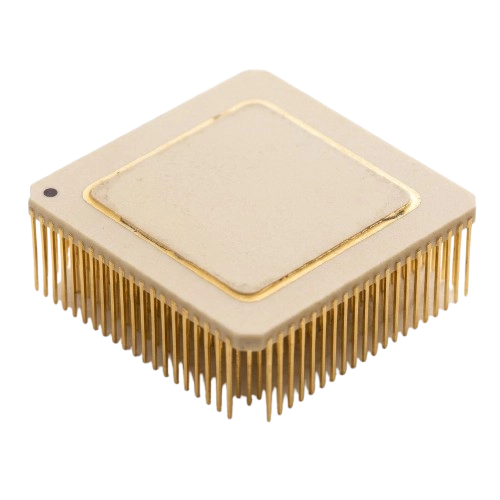
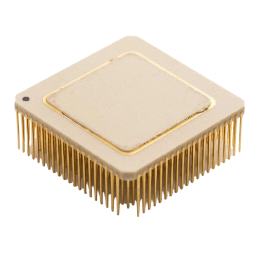
 XC2S30-6CS144C198 покупалиBGAВ наличииDatasheet
IC FPGA 92 I/O 144CSBGA ALIAS: XC2S30-6CSG144C
Ориентировочная цена$5.15
Частые вопросы
FAQ по товару
Точные ответы для покупателей, которые проверяют ordering code XC2S100-5FG256C, упаковку, наличие, datasheet и путь замены.
Что означает XC2S100-5FG256C?
XC2S100-5FG256C — это точный ordering code для компонента категории Embedded - FPGAs (Field Programmable Gate Array) от Xilinx. Текущий корпус указан как BGA, а контекст позиции включает IC FPGA 176 I/O 256FBGA. Используйте полный код при запросе склада, цены, datasheet или compliance-подтверждения.
Как покупателям проверить ordering code XC2S100-5FG256C?
Рассматривайте XC2S100-5FG256C как полный ordering code при RFQ и инженерной проверке. Подтвердите указанный корпус BGA, документацию производителя Xilinx, ordering table в datasheet, reel или packing details и требования внутреннего утверждения до замены или выпуска PO.
В каком корпусе поставляется XC2S100-5FG256C?
XC2S100-5FG256C сейчас указан с корпусом BGA от Xilinx. Перед утверждением закупки подтвердите manufacturer package drawing, footprint, pinout, tape-and-reel данные и требования к приемке.
XC2S100-5FG256C есть в наличии у TrustCompo?
На этой странице сейчас показано 1 публичные складские записи для XC2S100-5FG256C с указанным количеством 1 шт. Перед заказом подтвердите корпус (BGA), нужное количество, live availability, срок поставки, финальную цену, date code, MOQ, упаковку и документы RFQ.
Где сравнить альтернативы для XC2S100-5FG256C?
Для XC2S100-5FG256C сейчас не опубликован список связанных альтернатив. Отправьте RFQ с количеством, ограничениями по корпусу и требованиями к утверждению, чтобы TrustCompo помогла проверить возможные replacement options.